
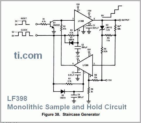
LF398 – Monolithic Sample and Hold Circuit
The LF198/LF298/LF398 are monolithic sample-and-hold circuits which utilize BI-FET technology to obtain ultra-high dc accuracy with fast acquisition of signal and low droop rate.
Operating as a unity gain follower, dc gain accuracy is 0.002% typical and acquisition time is as low as 6 µs to 0.01%. A bipolar input stage is used to achieve low offset voltage and wide bandwidth. Input offset adjust is accomplished with a single pin, and does not degrade input offset drift.
The wide bandwidth allows the LF198 to be included inside the feedback loop of 1 MHz op amps without having stability problems. Input impedance of 1010Ohm allows high source impedances to be used without degrading accuracy.
P-channel junction FET’s are combined with bipolar devices in the output amplifier to give droop rates as low as 5 mV/min with a 1 µF hold capacitor. The JFET’s have much lower noise than MOS devices used in previous designs and do not exhibit high temperature instabilities. The overall design guarantees no feed-through from input to output in the hold mode, even for input signals equal to the supply voltages.