
Successful PCB Grounding – Mark Fortunato
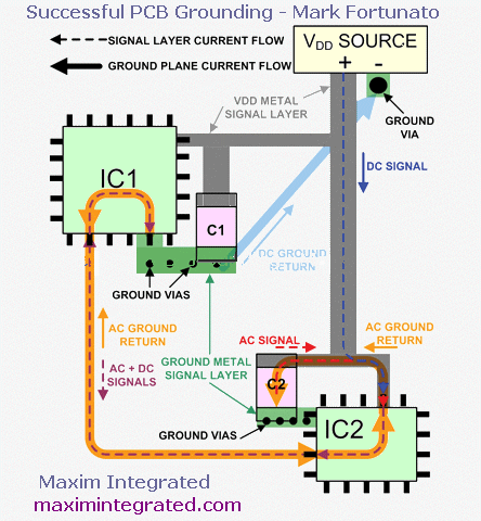
This tutorial discusses proper printed-circuit board (PCB) grounding for mixed-signal designs. For most applications a simple method without cuts in the ground plane allows for successful PCB layouts with this kind of IC.
“Ground Is Not an Equipotential – At this point it is important to understand that a ground plane, despite what we were taught it EE101, is not an equipotential. First of all, no matter how thick the copper is for your ground plane, it does have resistance. Therefore, if the analog and digital return currents (or any two currents) share a portion of the ground plane (i.e., their currents flow through the same metal) there will be crosstalk between the two as the copper resistance causes IR voltage drops.”
Successful PCB Grounding – Mark Fortunato
“With the basics of current flow on a PCB understood, we can start using this knowledge to properly handle the grounding of mixed analog-digital ICs. Ultimately, the goal is to ensure that the digital and analog currents do not share portions of the same return path.”
“Many problems with mixed-signal PCB design can be avoided by following this simple advice: pay attention to where the current flows. For most cases all we have to do is remember two basic principles: DC and low frequencies flow mostly in the straight-line path of least resistance between source and load; and high-frequency signals follow the path of least impedance, which is directly under the signal trace. In-between frequencies flow by both paths and in between the two paths.”