
The MOSFET in Power Electronics
delabs Notes – In a Circuit Module, if all Power and Signal Polarities are reversed. All NPN to PNP, All N-Channel to P-Channel and
Vice Versa. All Diodes and Caps too turned around. This Topsy Turvy or Mirror Design ought to work in Theory. It has worked for some circuits in practice too in my experience. ?
Some believe that N-Channel is more Robust than the P Type. In Bipolar Transistor NPN is more trusted for the final output stages. The NPN Transistor and N-Channel turn-on by a Positive control bias. It may be inappropriate to say this mosfet is NPN or PNP.
The traditional metal–oxide–semiconductor (MOS) structure is obtained by growing a layer of silicon dioxide (SiO2) on top of a silicon substrate and depositing a layer of metal or polycrystalline silicon (the latter is commonly used). As the silicon dioxide is a dielectric material, its structure is equivalent to a planar capacitor, with one of the electrodes replaced by a semiconductor.
Power Electronics & Energy Systems
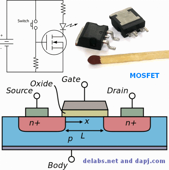
If the MOSFET is an n-channel or nMOS FET, then the source and drain are “n+” regions and the body is a “p” region. If the MOSFET is a p-channel or pMOS FET, then the source and drain are “p+” regions and the body is a “n” region. The source is so named because it is the source of the charge carriers (electrons for n-channel, holes for p-channel) that flow through the channel; similarly, the drain is where the charge carriers leave the channel. MOSFET – Wikipedia